최근검색어


OVERVIEW
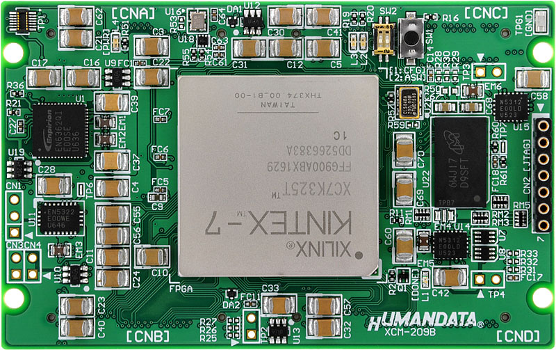
XCM-209 is an evaluation board equipped with a XILINX's high performance FPGA, Kintex-7 series (FFG900 package).
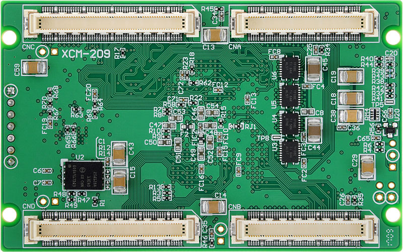
XCM-209 has voltage regulators, an oscillator, user LEDs, switches and a configuration device on its compact credit-card size board.
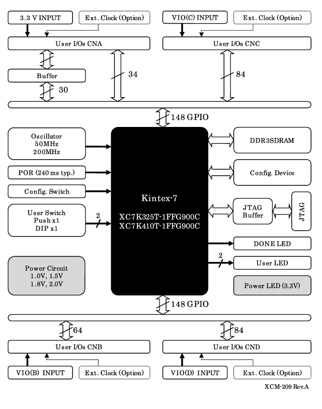
Only one 3.3V single power supply is needed. There are 296 user I/Os divided into four Vcco groups.
Vivado Design/System license is required to develop this board.
The free "WebPack" version does not support the FPGA device of this board.
BLOCK DIAGRAM
SPECIFICATIONS
- Xilinx Kintex-7
- XC7K325T-1FFG900C
- XC7K410T-1FFG900CFeature XC7K325T XC7K410T Logic Cells 326,080 406,720 Slices 50,950 63,550 Maximum Distributed RAM (kb) 4,000 5,663 Maximum Block RAM (kb) 16,020 28,620 DSP Slices 840 1,540 CMT (MMCM x1 + PLL x1) 10 10 Maximum user I/O pins (Device) 500 500 Maximum user I/O pins (Board) 296 296
- User I/O : 296 (HIROSE connectors, 80 pin x2, 100 pin x2)
- IOA (CNA Connector) : 64
(Some of the IOA are connected HP bank with level conversion ICs.)
- IOB (CNB Connector) : 64
- IOC (CNC Connector) : 84
- IOD (CND Connector) : 84 - Separated Vcco input for each connector
- IOA : Fixed to 3.3V input from CNA Connector
- IOB : External input from CNB Connector
- IOC : External input from CNC Connector
- IOD : External input from CND Connector - DDR3 SDRAM
Micron: MT41K64M16 (Micron, 1Gbit) - Configuration Device
Quad SPI ROM: N25Q128 or N25Q256 (Micron, 128/256Mbit) - JTAG port (7 pin socket)
- JTAG buffer for stable download and debug - Power : 3.3V single supply
- 1.0V/1.5 V/1.8 V/2.0 V on-board regulators
- Sequenced power supplies (Power on) - on board clocks
- 50 MHz (LVTTL)
- 200 MHz (LVDS) - Power-on Reset IC for FPGA configuration
- User Switch : 2 (Push x1, DIP x1bit)
- User LED : 2
- Status LED : 2 (Power, Done)
- High quality ten layers PCB. (Immersion gold)
- Credit-Card-Size 3.386"x 2.126" (86 x 54 mm)
- Tested all I/O
- RoHS compliance
- MADE IN JAPAN
PACKAGE CONTENTS
| Item | Image | Quantity |
|---|---|---|
| FPGA board (XCM-209-***) |  | 1 |
| Sockets (HIROSE 80P) |  | 2 |
| Sockets (HIROSE 100P) |  | 2 |
There is no paper document such as user's manual and circuit schematic in the package.
Please download those documents from the link in the documentation section below.